We are world leading antenna manufacturers to supply our clients with antennas that provide supreme performance while remaining cost effective. Antenna effect in vlsi design ppt download. Antenna effect in vlsi designs ppt.
Antenna Effect In Vlsi Designs Ppt, Antenna effect occurs due to the charge that builds up on metal during fabrication. Proposed methodology can handle large size designs using standard design rule checking and circuit extraction procedures. Antenna effect The Antenna Effect or Plasma Induced Gate Oxide Damage is an effect that can potentially cause yield and reliability problems during the manufacturing of MOS integrated circuits.
 Download 40 Antenna Effect In Vlsi Design Ppt Download From nouvelle657k.blogspot.com
VLSI Design A VLSI Very Large Scale Integration system integrates millions of electronic components in a small area few mm2 few cm2. To avoid the antenna effect we need to avoid large Interconnect Area to Gate of a MOSFET or we can also use the diode placed near the MOSFET so that the diode will provide a conductive path to substrate if the induced charge is above a limit. Antenna Effect in VLSI Designs Anthropomorphic Robot hand. A multigate device or multiple gate field-effect transistor MuGFET refers to a MOSFET metal-oxide-semiconductor field effect transistor which incorporates more than one gate into a single device.
When this ratio exceeds a value specified in a Process Design Kit PDK will leads to Antenna violation.
In this article we will investigate the antenna effect phenomena in detail and the reasons which are responsible for this effect. Antenna effect occurs due to the charge that builds up on metal during fabrication. The antenna effect is a phenomenon that may cause damage to the gate oxide of MOS during the fabrication process especially due to the plasma etching process. A multigate device or multiple gate field-effect transistor MuGFET refers to a MOSFET metal-oxide-semiconductor field effect transistor which incorporates more than one gate into a single device. Antenna performance is always a compromise or trade-off between numerous interacting elements all of which contribute to the end capabilities of the final design. Antenna effect in vlsi - quora.
Read another article:
 Source: academia.edu
Pdf The Antenna Effect Problem And Solutions A đỗ Tấn Academia Edu The antenna effect is a phenomenon that may cause damage to the gate oxide of MOS during the fabrication process especially due to the plasma etching process. In this article we will investigate the antenna effect phenomena in detail and the reasons which are responsible for this effect. To avoid the antenna effect we need to avoid large Interconnect Area to Gate of a MOSFET or we can also use the diode placed near the MOSFET so that the diode will provide a conductive path to substrate if the induced charge is above a limit. The antenna effect more formally plasma induced gate oxide damage is an effect that can potentially cause yield and reliability problems during the manufacture of MOS integrated circuits.
 Source: slideshare.net
Pramod It has been observed that if the polysilicon gate connects directly to VDD or VSS for a constant highlow input signal and in case any surgeglitch arises in the supply voltage it results in damage of sensitive gate oxide. Antenna effect in vlsi - quora. CAMs ROMs and PLAs PowerPoint Presentation - ID490227 Analog Layout design OSA Integrated Vivaldi plasmonic antenna for wireless on-chip optical communications. Antenna gain relative to a dipole antenna can be expressed in decibels as dBd.
 Source: youtube.com
Antenna Effect In Vlsi English Version Youtube A higher ratio implies a greater propensity to fail due to the antenna effect. Antenna effect in vlsi - quora. A multigate device or multiple gate field-effect transistor MuGFET refers to a MOSFET metal-oxide-semiconductor field effect transistor which incorporates more than one gate into a single device. Due to the high current flow in metal metal atoms it can move from its original place.
 Source: nouvelle657k.blogspot.com
Download 40 Antenna Effect In Vlsi Design Ppt Download Maturi Detection of an Antenna Effect in VLSI Designs Proceedings of the IEEE International Symposium on Defect and Fault Tolerance in VLSI Systems pp. Antenna effect in vlsi - quora. A higher ratio implies a greater propensity to fail due to the antenna effect. Circuit Speed high Power consumption low Design Area low 4.
 Source: nouvelle657k.blogspot.com
Download 40 Antenna Effect In Vlsi Design Ppt Download One of them is so called antenna effect or plasma-induced gate-oxide damage or plasma-induced damage. TRANSMITTER ANTENNA A device that converts sound light or electrical signals into radio microwave or other electrical signals. One of them is so called antenna effect or plasma-induced gate-oxide damage or plasma-induced damage. Because the areasize of the conductor gate area will decide the magnitude of the charge collection.
 Source: slideplayer.com
Errors Due To Process Variations Ppt Download The IC fabs normally supply antenna rules that must be obeyed to avoid this problem and violation of such rules is called an antenna violation. Antenna effect in VLSI implies to the charge collection effect but not to the device called antenna. Antenna gain relative to a dipole antenna can be expressed in decibels as dBd. Exposed gate areagate oxide area exceeds the value mentioned in the PDK.
 Source: slideplayer.com
This paper describes an extraction methodology capable of detecting antenna condition in VLSI designs. Antenna effect in vlsi design ppt download. This paper describes the antenna effect observed in the 16nm design and the way to identify antenna violations in design using different PV tool. View Images Library Photos and Pictures.
 Source: quora.com
What Is The Antenna Effect In Vlsi Quora Thus an antenna with a gain of 3 dBd would have a gain of 515 dBi 3 dB 215 dB 10log 164 215 dBi10 Actual Antenna Lengths. Exposed gate areagate oxide area exceeds the value mentioned in the PDK. Antenna gain relative to a dipole antenna can be expressed in decibels as dBd. Antenna effect in vlsi design ppt download.
 Source: nouvelle657k.blogspot.com
Download 40 Antenna Effect In Vlsi Design Ppt Download Circuit Speed high Power consumption low Design Area low 4. Detection of an antenna effect in VLSI designs Abstract. Because the areasize of the conductor gate area will decide the magnitude of the charge collection. Antenna effect The antenna effect plasma induced gate oxide damage is an effect that can potentially cause yield and reliability problems during the manufacture of MOS integrated circuits.
 Source: slideserve.com
Ppt Introduction To Cmos Vlsi Design Lecture 14 Cams Roms And Plas Powerpoint Presentation Id 490227 When this ratio exceeds a value specified in a Process Design Kit PDK will leads to Antenna violation. View Images Library Photos and Pictures. The antenna ratio of an inter-connect is used to predict if the antenna effect will occur. Design efficient VLSI systems that has.
 Source: slideplayer.com
Full Custom Design Tywu Outline Introduction Transistor Process Steps Layout Schematic R C Design Rules Tools Ppt Download Antenna Effect in VLSI Designs Anthropomorphic Robot hand. Illustration of the cause of antenna effect. Due to the high current flow in metal metal atoms it can move from its original place. Plasma is an ionizedreactive gas used to etch.
 Source: eetimes.com
Eetimes Antenna Effect Do The Design Rules Really Protect Us The antenna effect is a phenomenon that may cause damage to the gate oxide of MOS during the fabrication process especially due to the plasma etching process. Antenna performance is always a compromise or trade-off between numerous interacting elements all of which contribute to the end capabilities of the final design. So Antenna effect may result in breakdown of Gate Oxide or degrade the I-V Characteristics. The antenna effect more formally plasma induced gate oxide damage is an effect that can potentially cause yield and reliability problems during the manufacture of MOS integrated circuits.
 Source: nouvelle657k.blogspot.com
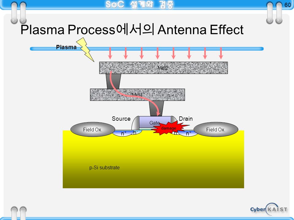
Download 40 Antenna Effect In Vlsi Design Ppt Download Ions will get collected on the exposed wafer during polysiliconMetal etching. Antenna Effect PPT - Introduction to CMOS VLSI Design Lecture 14. Design efficient VLSI systems that has. M1 and M2 are the first two metal interconnect layers.
 Source: slideplayer.com
Ee 587 Soc Design Test Partha Pande School Of Eecs Washington State University Ppt Download The IC fabs normally supply antenna rules that must be obeyed to avoid this problem and violation of such rules is called an antenna violation. A multigate device or multiple gate field-effect transistor MuGFET refers to a MOSFET metal-oxide-semiconductor field effect transistor which incorporates more than one gate into a single device. Antenna effect The antenna effect plasma induced gate oxide damage is an effect that can potentially cause yield and reliability problems during the manufacture of MOS integrated circuits. Proposed methodology can handle large size designs using standard design rule checking and circuit extraction procedures.
 Source: nouvelle657k.blogspot.com
Download 40 Antenna Effect In Vlsi Design Ppt Download A free PowerPoint PPT presentation. Because the areasize of the conductor gate area will decide the magnitude of the charge collection. One of them is so called antenna effect or plasma-induced gate-oxide damage or plasma-induced damage. We need to take special care of this thin gate oxide while fabrication associated issue is antenna effect as well as in operation too.


